What’s Pushing Solar Energy Efficiency?
From our post last week we visited some research at California Institute of Technology’s division of Chemical and Chemical Engineering The Lewis Group and its focus on energy conversion and trade-offs between costs and efficiencies for photovoltaic (PV) devices.
We are providing a brief and very oversimplified analysis of the physics behind solar energy, and to that end, an overview of semiconductor band gaps and new technological approaches to optimize solar energy conversion efficiency. Our prior discussions on energy conversion process, dealt with of the properties of various materials used in silicon and thin-film solar cells. (see Research at Caltech may provide clues to improving solar cell efficiency Energy bands and band gaps provide a way of understanding some of the limitation of solar energy efficiency.
Semiconductor Band Gaps
In semiconductors, the band gap refers to the separation between the valence band, where the electrons are shared among the atoms in the material, and the conduction band where electrons can travel. When the material absorbs light, the electrons, when excited to the band gap threshold level, are able to jump to the conduction band and in the process, create electrons and positively charged holes, that in turn generate electric current.
The energy bands refer to the large number of tightly spaced energy levels associated with crystalline materials. Because electrons behave in wave like movements, their movement interferes with neighboring atoms. The physical properties of semiconductor material are much then those of metals. The minimum energy required to free an electron in metal, ( photo-electric effect) is significantly less than that of semiconductors. For metals the energy bands are more or less continuous, the valence band and the conductive band overlap.
In semiconductor materials such as crystalline, energy bands are grouped into bands, hence energy bands. In crystalline material, the energy bands are split between an upper band called the conductive band and a lower band called the valance band. The energy band gaps in photovoltaic semiconductors are different depending upon materials used. The separations of energy bands in crystalline materials results in gaps between the energy bands and are referred to as the energy band gaps. There are discrete and direct band gap materials. Direct band gap refers to having the conductive band minimum energy value and the maximum valance band energy at the same value such as metals. Please see Bart Van Zeghbroeck’s Principles of Semiconductor Devices chapter 2 for a review of energy bands and semiconductor band gaps.
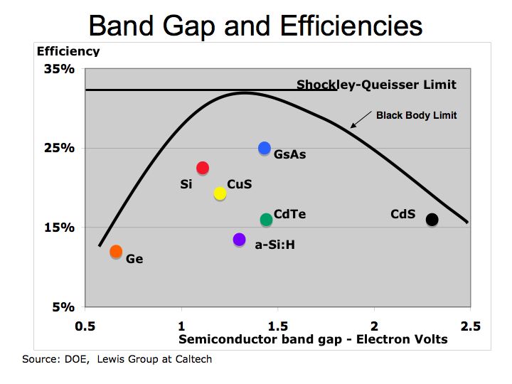
Figure 1 Semiconductor Band Gaps
With a host of physics equations, models, functions, and laws, one can calculate the energy band gaps for semiconductor materials. In addition, one can alter the band gap of the material through, heat, pressure, or introducing impurities into the material (doping the material) to change its physical properties. In general, the more direct the band gap, the more efficient the band gap material. However, research is working processes to improve efficiencies through doping the material and introducing new materials. The processes seek to narrow the band gap of the semiconductor and thereby improve their efficiencies.
One must remember the cost efficiency tradeoff in evaluating which semiconductor material is best in achieving efficiency and cost parameters. Again, the Shockley-Queisser limit of approximately 30%-to-32% for single junction solar cell and a thermodynamic limit of about 83% are also constraint to improving solar energy efficiency. Please see “Detailed Balance Limit of Efficiency of p-n Junction Solar Cells” (W Shockley and HJ Queisser, Journal of Applied Physics, 1961). Semiconductor materials have limited efficiency because excess photon energy generates heat and not electric current.
Research studies on improving solar energy efficiency are embracing numerous fronts including concentrators and multi-junction semiconductors to impact ionization and spectral conversion. For a quick review, please Imperial College, Jenny Nelson’s Third generation Solar Cells. Multi-junction semiconductors employ two or triple junction semiconductor material to capture excess photon energy. A good overview on solar energy is presented by the DOE’s National Renewable Energy Lab (NREL) Third Generation Solar Photon Conversion (Exceeding the 32% Shockley(Exceeding the 32% Shockley—Queisser Limit)
Figure 2 Approaches to PV Cell Efficiency
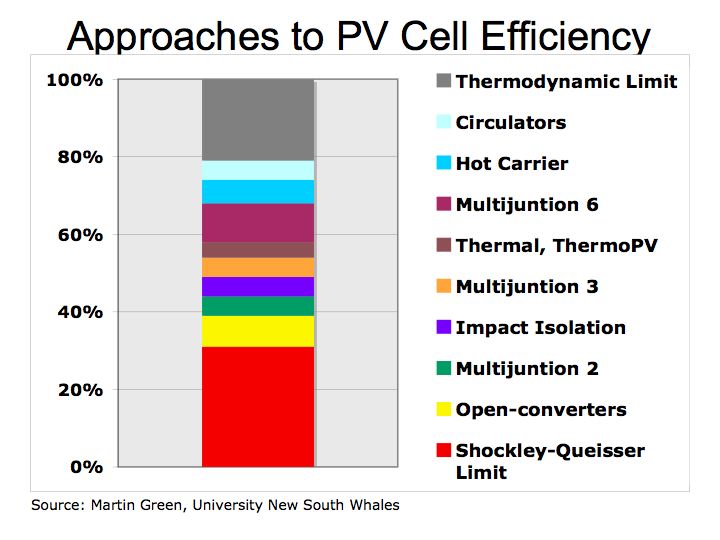
There should be considerable excitement given the potential that greater efficiency should be able to drive solar energy costs lower. With PV cells below $3.00/watt (or $0.15/ kilowatt-hour), solar energy with be close to parity with conventional electric rates which are about $0.11/KWH. The bottom line is innovative research has the potential to offer the disruptive technology that significantly changes the economics of delivering an energy solutions to all nations.
canapé
Great blog you have here.. It’s hard to find quality writing like
yours these days. I seriously appreciate individuals like you!
Take care!!